- ▶ Focusing on High-End Substrate Markets such as Servers and Autonomous Driving with Industry-Leading FCBGA Technology
- - Plan to secure more than 50% proportion of high value-added FCBGA products such as servers, AI, automotive, and networks within two years
- - Equipped with a triple-threat of 30 years of accumulated technology, around 2 trillion KRW large-scale investment, and market growth potential
- - Implemented ultra-gap technology with mass production at new factories in Busan and Vietnam
- - New plant in Vietnam features a smart factory system with an intelligent manufacturing system based on AI deep learning technology
- ▶ Semiconductor Substrate Market to Grow from 4.8 Trillion KRW in 2024 to 8 Trillion KRW by 2028
- - Market growth driven by industries such as 5G antennas, ARM CPUs, and servers/automotive/networks
Samsung Electro-Mechanics has introduced high-performance FCBGA, and plans to increase the proportion of high-value FCBGA products for servers, AI, automotive, and networks to over 50% by 2026.
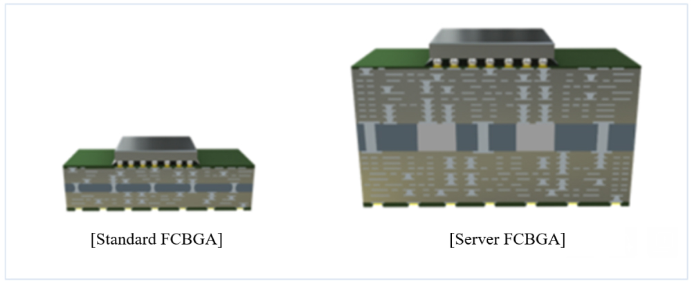
In July, Samsung Electro-Mechanics announced that it had signed a high-performance computing (HPC) server FCBGA supply agreement with global semiconductor company AMD and has begun mass production of the products. Server FCBGA is the most technically challenging among semiconductor substrates, and only a few global companies are capable of mass production of high-end server substrates. Server CPUs and GPUs require multiple semiconductor chips to be installed on a single substrate to accommodate high performance such as improved processing power and signal speed. Therefore, server FCBGA substrates are more than four times the size of standard FCBGA for PCs and have more than twice the number of layers, exceeding 20 layers. As such, server FCBGA requires advanced manufacturing technology and dedicated facilities to enhance product reliability and production yield due to the large size of the substrate and high number of layers, making it a challenging field for new entrants.
Samsung Electro-Mechanics is maintaining its ultra-gap technology in the semiconductor substrate field through a large-scale investment of 1.9 trillion KRW, operating its new factories in Busan and Vietnam as high-end product mass production bases. In particular, the Vietnam factory is implementing a smart factory system with an intelligent manufacturing system based on automated logistics and advanced manufacturing environments to ensure stable production.
Samsung Electro-Mechanics automatically collects and analyzes all operational data in the factory through its intelligent manufacturing system, reflecting it in real-time on the production lines. In addition, the Vietnam factory uses AI deep learning technology to automatically apply optimal recipes and conducts real-time analysis based on data to produce products of the highest quality.
Samsung Electro-Mechanics is leading the substrate industry by supplying products to top global companies with differentiated technology and strengthening cooperation with customers by securing key technologies for next-generation semiconductor substrates.
Since successfully mass-producing server FCBGA for the first time in Korea in October 2022, Samsung Electro-Mechanics has been recognized for its industry-leading FCBGA technology. Samsung Electro-Mechanics is focusing on high-end semiconductor substrate markets such as high-performance servers and networks, and autonomous driving, planning to secure over 50% share of high-value FCBGA products by 2026.
- ▶ Semiconductor Substrate: The Nerve and Blood Vessel of Our Body
- - Semiconductor = Brain, Semiconductor Substrate = Bones, Nerves, and Blood Vessels
- - The link between semiconductor chips and the main substrate
The semiconductor substrate plays a role in transmitting electrical signals between semiconductors and main substrates and protecting the semiconductor from external impacts, etc.
If semiconductor chips are likened to the brain, the semiconductor substrate can be compared to the bones protecting the brain as well as the nerves and blood vessels that transmit information from the brain to various organs.
Semiconductor chips need to be connected to the main substrate, but the circuits on the main substrate cannot be made as finely as those on the semiconductor. The distance between the terminals of a semiconductor chip is 100 micrometers (µm), roughly the thickness of an A4 paper, while the distance between terminals on the main substrate is about 350 µm, roughly four times different.
Thus, a semiconductor substrate acts as a bridge connecting the semiconductor chip and the main substrate.

- ▶ “1/20 the Thickness of a Human Hair,” FCBGA: The Pinnacle of Micro Technology
- - As electronic devices become more functional, circuit line widths decrease and internal layers increase
- - Samsung Electro-Mechanics holds world-class micro-processing & microcircuit technology
FCBGA (Flip-Chip Ball Grid Array), a type of semiconductor substrate, connects high-integrated semiconductor chips and substrates using flip-chip bumps, enhancing electrical and thermal characteristics. It is mainly used in CPUs (Central Processing Units) and GPUs (Graphics Processing Units) for PCs, servers, networks, and automobiles.
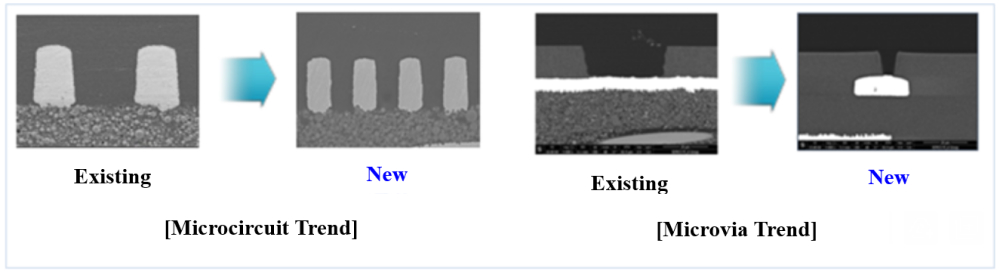
The key technologies needed to manufacture semiconductor substrates are “fine processing technology” and “microcircuit implementation.” As electronic devices increase in functionality, more components are needed, leading to more and more complex paths for signal transmission, i.e. circuits. To create many paths (circuits) within a limited substrate area, multiple layers such as 4-layer, 6-layer, 8-layer, or 10-layer substrates are used. Therefore, vias, or holes connecting layers, must be precisely drilled and plated to ensure electrical connections. The vias, generally about 80 µm in size, need to be drilled accurately to 50 µm without errors, requiring sophisticated processing technology. Samsung Electro-Mechanics can implement vias as small as 10 µm, or 1/10 the thickness of an A4 paper, showcasing world-class microvia formation technology.
Circuit paths, through which electrical signals pass, are becoming finer as the number of terminals and signals increases. The manufacturing process involves coating the areas left over after plating with the desired circuit thickness and then using chemical processes (etching) to form only the required circuits. Achieving a circuit line width and spacing of 8-10 µm is a challenging technology. As the number of semiconductor input/output terminals increases, even finer circuit implementations are needed. Samsung Electro-Mechanics possesses microcircuit formation technology capable of creating circuit line widths as small as 5 µm, or 1/20th the thickness of a human hair.
- ▶ Semiconductor Package Substrates Emerging as Key Components for Enhancing Semiconductor Performance
- - Increased importance of package solutions to overcome semiconductor miniaturization limits
- - Advancing substrate technology required due to multi-package trends
- - Package substrate market expected to reach 8 trillion KRW by 2028, with an annual growth rate of 14%
- - Market growth driven by industrial and automotive fields such as 5G antennas, ARM CPUs, and servers/automotive/networks
In the past, semiconductor chips had a simple structure with one semiconductor chip placed on a substrate. However, to enhance semiconductor performance, miniaturization of circuits and a geometric increase in transistor count have been pursued.
Although technologies like EUV processes are developed for miniaturization, the limitations of miniaturization technology and rising process costs due to expensive equipment raised semiconductor costs and have increased the need for improving semiconductor performance and reducing costs in post-processing, such as packaging.
In addition, while chip manufacturing quality was once the primary focus, recent trends emphasize how well the product is assembled into a high-quality final product. In other words, multi-package products, which enhance overall functionality by mounting various semiconductor chips on a substrate, are emerging. This requires finer circuit patterns on the substrate, larger substrate areas, and increased layer counts, leading to advancements in semiconductor substrate technology.
According to market research firm Prismark, the semiconductor substrate market is expected to grow from 4.8 trillion KRW in 2024 to 8 trillion KRW by 2028, with a projected annual growth rate of about 14%. In particular, market growth is anticipated to be driven by industrial and automotive fields such as 5G antennas, ARM CPUs, servers/automotive/networks.
The semiconductor industry urgently needs substrate technologies capable of meeting the demands of robotics, metaverse, autonomous driving, and other applications requiring enhanced semiconductor performance. FCBGA, used in big data and AI, especially demands high technology for larger sizes, increased layers, microcircuit implementation, and material convergence.
- ▶ Samsung Electro-Mechanics Maintains Ultra-Gap with Differentiated Semiconductor Substrate Technology
- - Samsung Electro-Mechanics strengthens global customer partnerships with 30 years of accumulated super gap technology
- - Technologies include ultra-large area technology over 110 mm, ultra-thick layers with more than 26 layers, and EPS technology that integrates passive component parts
Samsung Electro-Mechanics leads the substrate industry by supplying products to the world’s leading companies with its differentiated technology. In particular, Samsung Electro-Mechanics is strengthening cooperation with customers by securing the element technologies needed in the next-generation semiconductor substrate market, such as expanding its ultra-large area technology over 110 mm, ultra-thick layer technology with more than 26 layers, and EPS technology, which expands the technology of embedding passive components in the package substrate to double the performance of semiconductors, and technology that implements ultra-fine circuits directly on the substrate to mount diverse silicon devices on a single package substrate to double the performance, etc.
Since starting the substrate business in 1991, Samsung Electro-Mechanics has led the industry by supplying products to top global companies with its differentiated technology. It holds the top position in the high-spec mobile AP semiconductor substrate market in terms of share and technology. With increasing demand for high-performance semiconductors due to AI technology, the demand for FCBGA is also expected to rise. As the first domestic company to mass-produce server FCBGA, Samsung Electro-Mechanics is focusing on developing next-generation substrates and strengthening competitiveness in the semiconductor substrate business.